PM Modi Launches Phase 2 of India Semiconductor Mission with ₹1.27 Lakh Crore Outlay
Prime Minister Narendra Modi inaugurated the fifth edition of SEMICON India 2026 at Yashobhoomi in New Delhi, officially launching Phase 2 of the India Semiconductor Mission (Semicon 2.0). Formally backed by an approved budgetary outlay of ₹1.275 lakh crore ($13.5 billion), the expanded policy framework signals a strategic shift from establishing pilot packaging units to scaling up commercial fabrication and building an integrated domestic semiconductor value chain.
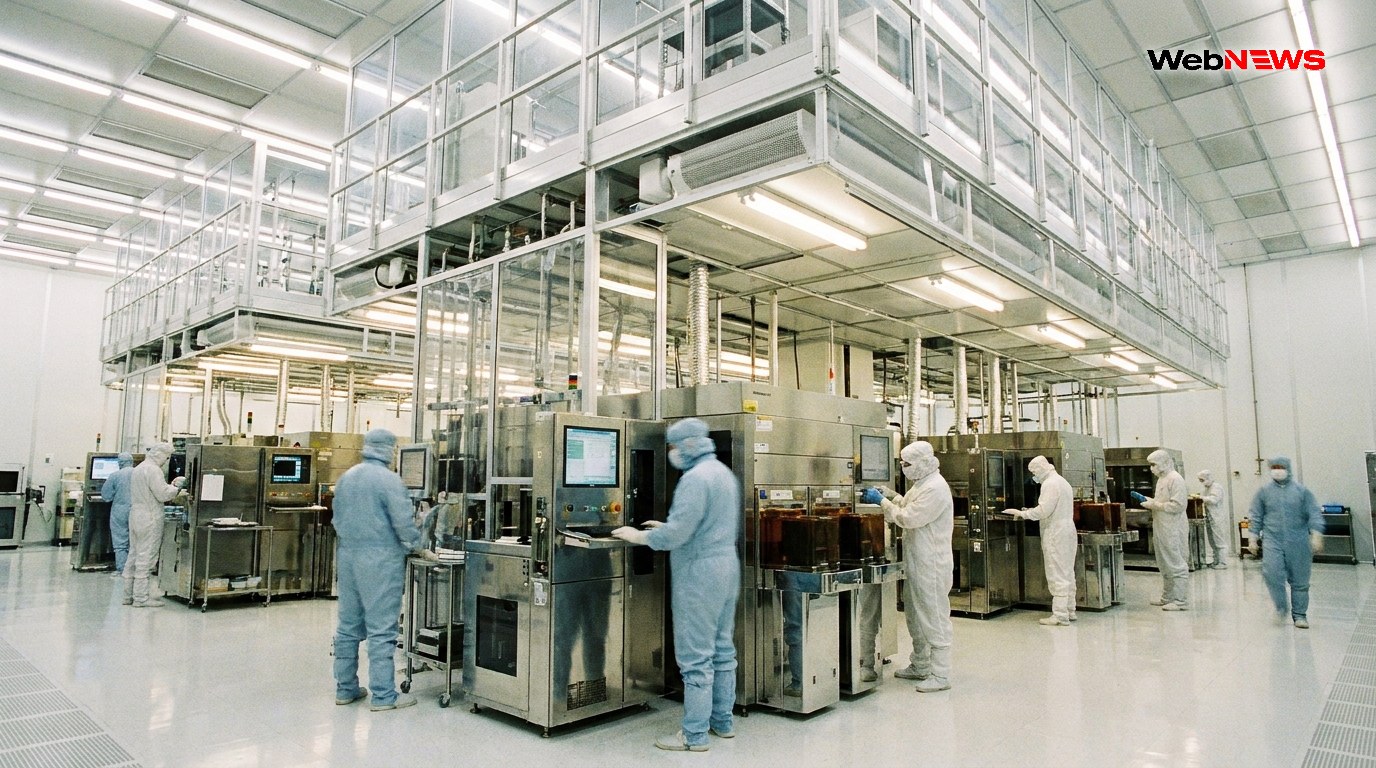
Semicon 2.0 is structured around six core operational pillars: fabless chip design, equipment and materials supply chains, commercial fabrication units, advanced packaging (ATMP/OSAT), applied research and development, and large-scale workforce talent development. During his address on September 17, 2026, PM Modi highlighted that India has achieved significant structural progress within four years that conventionally takes other nations decades. As part of the launch, commercial production lines were virtually commissioned at CDIL Semiconductor in Mohali, Punjab, and Suchi Semicon in Surat, Gujarat, expanding the country’s operational commercial semiconductor packaging facilities to five.
Under the updated policy guidelines, foreign technology firms are permitted to partner with domestic startups, design houses, and Overseas Citizen of India (OCI) owned enterprises to foster intellectual property creation within India. The government aims to generate nearly one lakh high-skilled engineering jobs and build a trained workforce of 100,000 technicians for cleanroom operations. Furthermore, the initiative targets financial and infrastructural backing for over 200 chip-design startups. The three-day global summit brought together over 600 participating companies and delegations from 52 countries, reflecting international investor confidence in India's technology ecosystem.